Q2
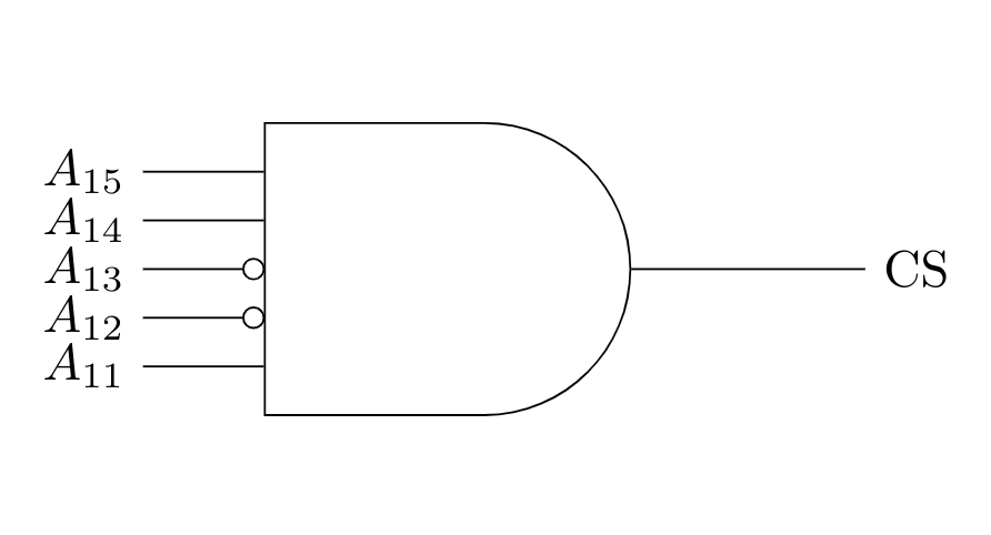
MCQ1 mark, −0.33The chip select logic for a certain DRAM chip in a memory system design is shown below. Assume that the memory system has address lines denoted by to . What is the range of address (in hexadecimal) of the memory system that can get enabled by the chip select (CS) signal?
Sign in to save attempts.
Loading…